Welcome to the analog-tutorials wiki!
This wiki covers getting started with open-source analog IC design tools. The basic flow is xschem for schematic capture, simulation, and SPICE netlist generation, then KLayout for layout.
Start by setting up the IIC-OSIC-TOOLS container, following the Setting Up Open Source Tools with Docker tutorial.
Pages
Once your environment is set up, work through the following examples, taking each block from schematic to layout:
Literature recommendations
- Practical Electronics for Inventors by Paul Scherz
- Fundamentals of Microelectronics by Behzad Razavi
- CMOS VLSI Design, A Circuits and Systems Perspective by Neil H. E. Weste and David Money Harris
- Open Circuits: The Inner Beauty of Electronic Components by Windell Oskay
- AIC2023 — and other years (e.g. AIC2026) — teaches core analog IC concepts while building circuits on the SKY130 PDK
Associated
- Xschem editor commands
- Basic operations on KLayout
- Terminology overview
- Learn Linux with Bandit
- Test Verilog and Digital Logic with EDA Playground
- Awesome open source ASIC resources
Inverter: Schematic to Layout
This page walks through building a basic CMOS inverter in xschem, simulating it, and then laying it out in KLayout. By the end you'll have a working schematic, a passing DC/transient sim, and a DRC-clean layout ready for LVS.
Overview
The inverter is the simplest CMOS logic gate and a good first exercise for the full analog flow: schematic capture in xschem, SPICE simulation with ngspice, and layout in KLayout. Working through it end-to-end will introduce you to PDK device symbols, sizing conventions (W/L ratios), and the basic layout rules you'll reuse in every later block.
Prerequisites
- IIC-OSIC-TOOLS container set up and running
- In this tutorial we'll be using the SKY130PDK
Steps
- Open the terminal (it should auto be in the directory
/foss/designs) and run the following:
sak-pdk SKY130A
xschem
- Click the
+symbol to open up a new schematic. You should now have a blank slate titleduntitled.sch - Right click -->
Insert symbol--> Place an NMOS and PMOS device from the PDK symbol library
File -> Save as -> inverter.sch
- Wire the gates together as the input, and the drains together as the output. Tie the PMOS source to VDD and the NMOS source to VSS
Ctrl + P or Symbol --> Place schematic input port
Ctrl + Shift + P or Symbol --> Place schematic output port
Double click on pin or press q to open up properties. Change XXX with name.
-
Set device sizing (W/L) for the desired switching threshold. Here, we make PMOS 3x wider (so w=3) while NMOS w=1.
-
aorsymbol -> make symbol from schematicto make a symbol from schematic. Open a new schematic again, place your symbol. or Run a DC sweep and transient simulation in ngspice to verify switching behavior -
Export the schematic's layout view / open the corresponding cell in KLayout
-
Place and size the NMOS and PMOS layout devices
-
Route the input, output, VDD, and VSS connections
-
Run DRC to check the layout is rule-clean
# launch xschem with the sky130 PDK
xschem &

# after schematic is done, simulate with ngspice
ngspice inverter_tb.spice

# open the layout in klayout
klayout inverter.gds
Results
| metric | value |
|---|---|
| switching threshold (V) | — |
| rise time (ns) | — |
| fall time (ns) | — |
| DRC violations | 0 |
Checklist
- Schematic captures NMOS + PMOS with correct connectivity
- DC sweep shows correct switching behavior
- Transient sim shows clean rise/fall
- Layout matches schematic connectivity
- DRC clean
Ring Oscillator
A 5-stage ring oscillator on SKY130, from schematic to simulated frequency. This page doubles as the formatting reference: every construct the renderer understands is used somewhere below.
TL;DR: an odd number of inverters in a loop has no stable DC operating point, so it oscillates at roughly
f = 1 / (2 * N * t_pd). Five stages of the standard inverter lands near 1.2 GHz at tt.
Overview
The ring oscillator is the hello world of analog design: it needs correct device models, a working simulator, and nothing else. If this page simulates cleanly, your toolchain setup is good and every later tutorial will run.
Inline styles for reference: bold, italic, both, inline code, struck, and an external link to the SKY130 PDK docs.
Prerequisites
xschemandngspiceinstalled and on$PATH- SKY130A PDK with
$PDK_ROOTexported- built with
open_pdks - includes the
sky130_fd_prprimitives library
- built with
- Basic familiarity with SPICE netlists
Schematic
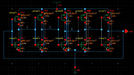
Keep the loop symmetric: identical W/L on every stage, and buffer the tap so the probe capacitance does not load the ring.
Netlist
* ring_osc.spice : 5-stage ring oscillator, sky130 tt
.lib $PDK_ROOT/sky130A/libs.tech/ngspice/sky130.lib.spice tt

.subckt inv in out vdd gnd
XM1 out in gnd gnd sky130_fd_pr__nfet_01v8 W=1   L=0.15
XM2 out in vdd vdd sky130_fd_pr__pfet_01v8 W=2.1 L=0.15
.ends

Xi1 n5 n1 vdd 0 inv
Xi2 n1 n2 vdd 0 inv
Xi3 n2 n3 vdd 0 inv
Xi4 n3 n4 vdd 0 inv
Xi5 n4 n5 vdd 0 inv

Vdd vdd 0 1.8
.ic v(n1)=0
.tran 10p 20n
.end
Run it
- Export the environment
export PDK_ROOT=/usr/local/share/pdk
- Launch the simulation
ngspice ring_osc.spice- wait for the transient to finish
- Measure the period on
v(n5)and invert it
Results
| Corner | VDD | f_osc | Power |
|---|---|---|---|
| tt | 1.80 V | 1.21 GHz | 84 uW |
| ss | 1.62 V | 0.89 GHz | 61 uW |
| ff | 1.98 V | 1.63 GHz | 118 uW |
Frequency tracks 1/t_pd, so expect roughly linear movement with VDD across corners.
Checklist
- schematic drawn, ERC clean
- transient runs at tt
- ss / ff corners swept
- layout drawn, DRC and LVS clean